
DDDAC I2S Interface
Introduction
Just a small in-between quick & dirty little project… It all started with a R2R DAC from Stefano, which was kindly sent to me for review, by Marcin. By the way…. there is a long thread about this Stefano DAC and the developments over time on the DIY Audio Forum: https://www.diyaudio.com/community/threads/italian-r2r-ladder-dac-no-cpid-dsp.390541/
Point is that this R2R DAC did not work well at my place. After some good support from Stefano, it turned out that his design demanded that the LR signal comes before the falling edge of BCK. Which is not always the case. Especially not in my WaveIO and AP2322 System two audio analyzer…

So, I needed to delay the LR signal a little bit. Two options:
- Fiddle around with some Inverter ICs, loosly wired kind of test thingie.
- Build something neat, which I can always use and is more universal….
Of course I took the second option. These days it is easier to quickly design a PCB and have a few produced & delivered within two weeks. And you cannot have enough Test and Measurement gear in your workshop, LOL!
As it might be interesting to read and may be for someone to build, I thought let’s post this…
If you want to build this yourself, just E-Mail me. I have a few PCBs left over (4x)
Functional Description
These were the design goals (which were met by the way)
- Two I2S inputs, selectable with a jumper or external switch
- I2S Inputs laid out to use with WaveIO – I still use Lucian’s board in my workshop as I2S source)
- Inputs compliant with 3,3- and 5-Volt logic
- Each signal (Data, LR, BCK) defined by jumper as “Inverted” or “Normal”
- Each Signal (Data, LR, BCK) has separate outputs with delays from 0 to 80ns in steps of 20ns
- Option for extra delay of BCK from 100ns – 180 ns (I did not install this yet – no real need)
This is the functional Block-Diagram, I think it is self-explanatory:

Here you see the ready board. It is not a masterpiece of PCB design, but it works great als workshop product. If you click on the picture, you will get the high-resolution image and you can zoom in at some details, like the delayed outputs and selectors.
There are also a few Test-Pads to hold on a probe for signal checking.

After arrival of the PCBs, I quickly soldered the PCB together and connected to the Stefano DAC. The 20ns delay for LR was already enough to have the DAC work properly and I could finally do some listening and AP2322 Tests. But that is not for this post to go into to.
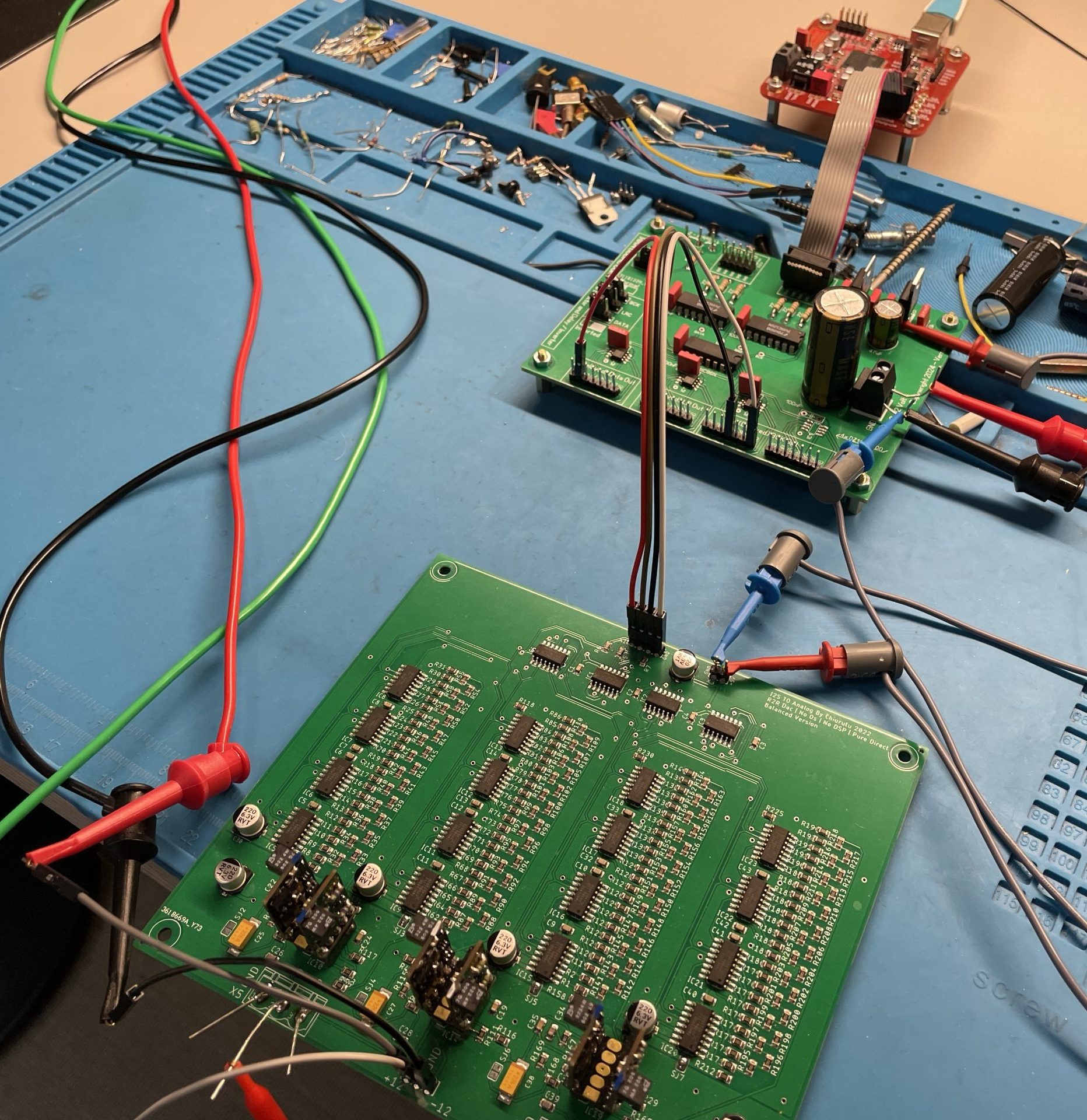
Here you see how the board is used.
WaveIO or AP-System connected to the input. Jumper to select input 1.
Signals “Normal”
Outputs (with BCK 20ns delayed) to the I2S input of the DAC. Power applied to the boards and ready to go testing and listening…
Conclusions
It was just fun to have a problem which resulted in the development of this simple tool. For the rest of my life, I can generate a wealth of different I2S signals for whatever test is on hand 🙂
If anyone is interested, let me know – just write me a mail. I have a few PCBs left… Happy to share (for DIY! My design cannot be used commercially, just as all DDDAC designs – just saying 😉 )